Bus breakout
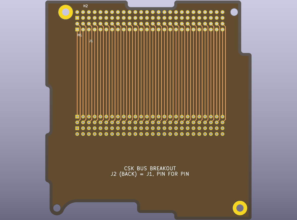
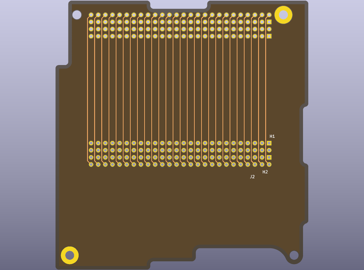
CSK_Bus_Breakout is a 4-layer board built from the Slot 0 template. J1 sits
on the stack position, and J2, a second H1/H2 header pair (CSK_PC104_Bus)
mounted on the bottom 38.1 mm below it, carries every bus pin, pin for pin.
Use it to reach the bus from below a stack, or as a starting point for a board
that needs a second bus connector.
Get it
From the releases page:
CSK_Bus_Breakout-fab-<version>.zip: Gerbers and drill files, ready to order;CSK_Bus_Breakout-<version>.zip: the KiCad project, with its own copy of the library.
In the repository it is breakout/.
Design
- Routing. Mounting J2 on the bottom mirrors its rows, so in each of the 26 columns the four tracks nest without crossing: H1's odd row drops straight down on F.Cu, and the other three rows each take the gap beside their column on one layer (F.Cu, In2.Cu, B.Cu). No vias; 0.25 mm tracks, 0.2 mm clearance, copper 1.27 mm from the edge.
- Ground. In1.Cu is a plane on the bus ground pins H2.29, H2.30 and H2.32
(
DGND), netGND. Every other net is named after its header pin,H1.1toH2.52, not its signal: each switchS0toS5has two terminals that share a name, and naming the nets by signal would short them. - Stackup. Generic 1.6 mm 4-layer: 35 µm copper on all layers, FR4.
- Checks. In KiCad 10.0.6: ERC clean; DRC 0 violations, 0 unconnected items, 0 schematic parity issues. CI checks this on every change.
Generated, not drawn
tools/genbreakout.py writes the board from the Slot 0 template and the
library (just breakout), so it follows them when they change.